Design Limits
Precision in Every Design
Pushing the boundaries of circuit board design, ensuring your projects meet the highest standards for performance and reliability.
Capabilities
Below lists what you can achieve working with Candor Industries. Rigid, rigid-flex, and flex circuit boards have the same design limits.

Minimum Trace Width
0.005"
0.003"/0.003"
0.002"/0.002"

Outer Layer Via Pad Size
Class 3: 2 Mil, and capable up to landless via
0.002"
0.002" high density drilling
Line to Line Spacing
0.005"
0.003"/0.003"
0.002"/0.002"
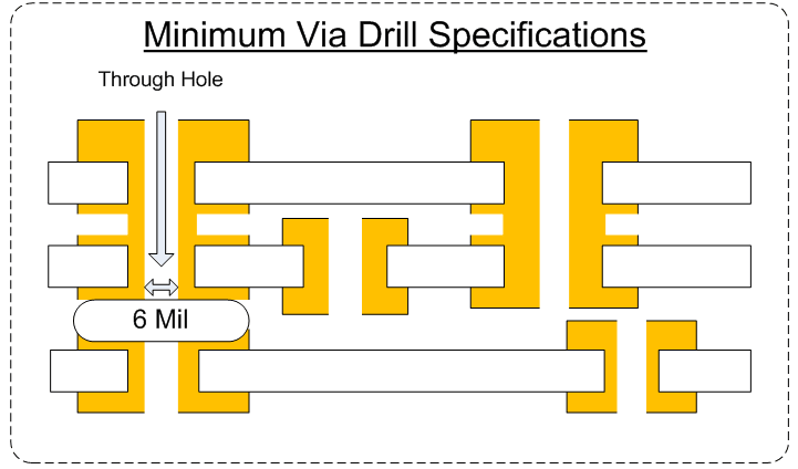
Minimum Through Hole Drilled
0.012"
0.008"
0.004"
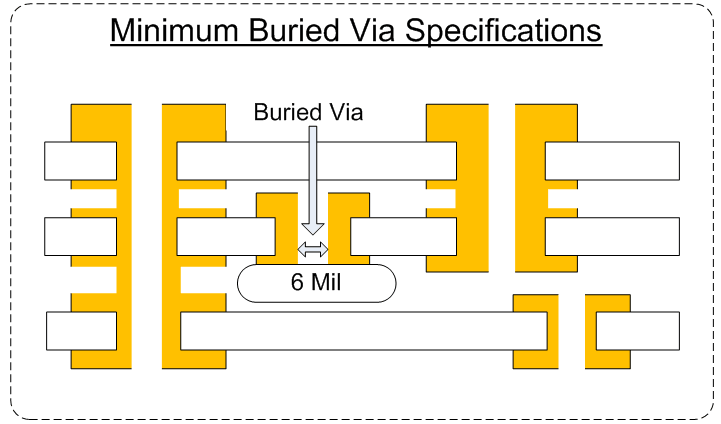
Minimum Buried Via Drilled
0.012"
0.006"
0.004"
Minimum Blind Via Drilled
0.012"
0.006"
0.004"
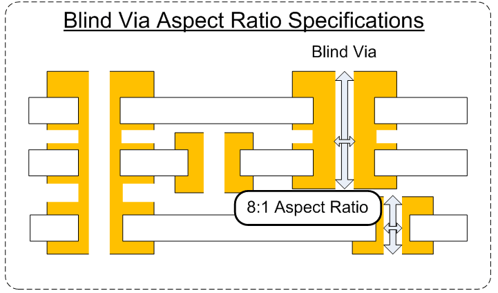
Blind Via Aspect Ratio
8:1 Aspect Ratio
1:1
1:1
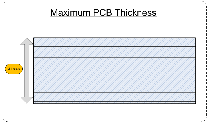
Maximum PCB Thickness
300 mil
0.008-0.125"
0.002"-0.4"
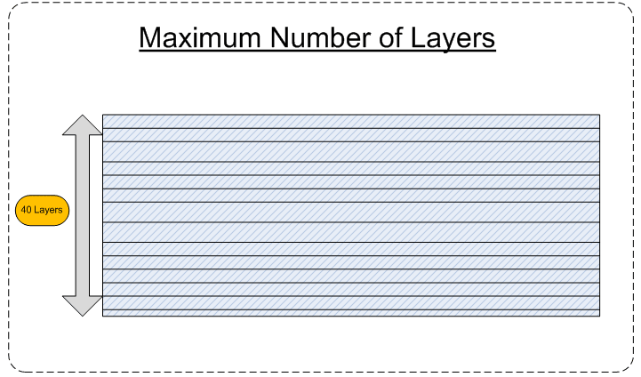
Number of Layers
12 Layers
22 layers
40 layers
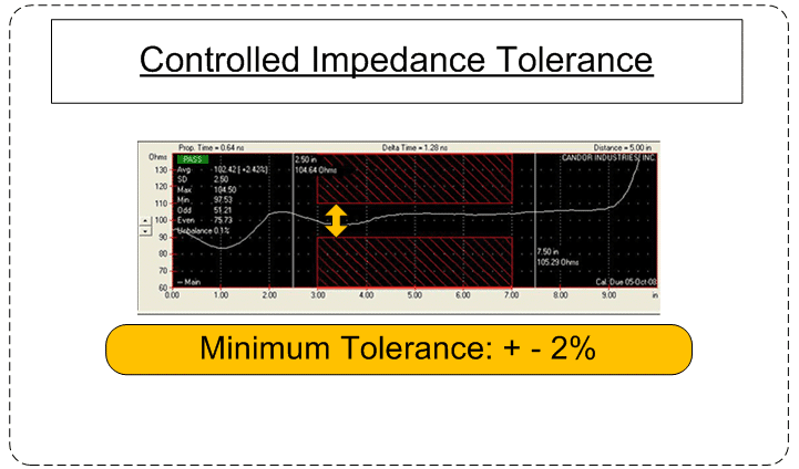
Controlled Impedance Tolerance
+- 5% or Under Tolerance
-0.05
-0.025

Maximum Board Size
19.5" X 22.5"
20.5 X 24.5"
20.5 X 26"
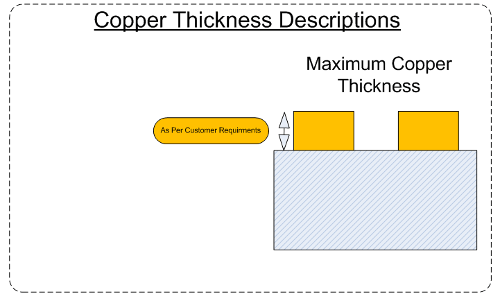
Copper Thickness/Density
Able to meet customer requirements.
.25-2oz
5microns-20oz
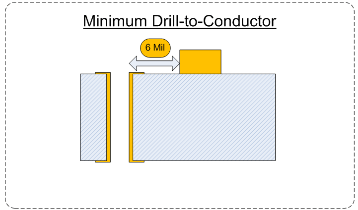
Minimum Drill-to-Conductor
6 Mil (edge of hole to track)
0.005"
0.003"
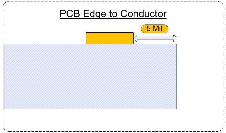
PCB Edge to Conductor
0.010"
0.005"
0.002"
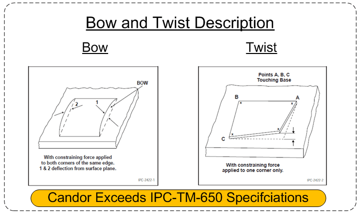
Warp (Bow and Twist)
Exceeds IPC-TM-650
exceeds IPC Spec
exceeds IPC Spec
Solder Mask DAM
0.010"
0.005"
0.002"