What is a PCB Assembler?
What is a PCB Assembler? A PCB assembler is an individual or company that builds electronic devices onto PCB. These professionals use techniques such as surface mount assembly (SMT), plated through-hole technology (PTH), and electro-mechanical assembly.
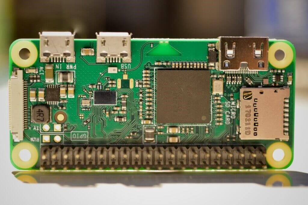
Photo by Gavin Allanwood on Unsplash
What Does a PCB Assembler Do?
A PCB (printed circuit board) assembler is either an individual or business tasked with building electrical products onto a PCB. In other words, their job is to carry out the process of PCB assembly, primarily by connecting the electronic device to the board via the designated wiring.
What is a PCB used for?
- Reading and comprehending wiring diagrams
- Following and replicating pathways illustrated on sample PCBs
- Selection of the appropriate electronic device for connection to the PCB
- The use of hand tools, such as soldering kits, in constructing and finishing the PCB
- Safe manipulation of wire leads (i.e., twisting, stripping, and bending, inserting color wires into corresponding holes, soldering, crimping, etc.)
- Press-fitting electronics onto the PCB
PCB assemblers most often work in the manufacturing and tech industries and come from all sorts of professional backgrounds, such as machine operators. Job titles you might have in this line of work include:
- Socket Assembler
- Pre-Wave Assembler
- Post-Wave Assembler
Learn more about the differences between PCB and PCBA .
What is the PCB Assembly Process?
The PCB assembly (PCBA) process requires high-tech machines, powered hand tools, and manual labor, all toward the goal of soldering a given electronic device onto its designated PCB. Throughout the process, you might enact a few quality control operations, such as:
- Solder paste inspection (SPI)
- Automated optical inspection (AOI)
- In-circuit testing (ICT)
Aside from these fail-safes, the main stages of the PCBA process are as follows:
- Before building any components onto the PCB, the assembler must apply solder paste to the sites at which the connections are to be installed. (Normally, this requires the application of the paste onto component pads using a solder screen.)
- Not all projects require solder paste. During wave soldering, for example, the paste is provided by the machine instead of manually applied by the assembler.
- After applying the solder paste, the board then transitions into the “pick and place” stage. At this point, a machine loads the necessary components and positions them onto their appropriate locations on the PCB.
- As the boards make their way out of the machine, the solder paste holds the components in place for the assembler to then solder. At this point, the assembler may use various solder machines, such as a wave soldering machine (although this practice is uncommon with the SMT method, discussed below).
- After the completion of this step, the assembler must inspect the board. You might carry out a manual or automatic inspection, depending on the process. (For example, SMT requires automated optical inspections due to the sheer number of components involved.)
- The assembler then tests the device and board to ensure the product is functioning correctly before distribution.
- Finally, the assembler may receive feedback for their work. Supervisors and others may provide feedback at the inspection stage to catch potential flaws more quickly.
What Are Various Ways to Create PCB Assemblies?
Throughout your career, you may use several different techniques to carry out the PCBA process. Each method is distinct for its capacity to manage board complexity, execute specific building and assembly techniques, and more. Below are some of the most widely accepted practices.
Surface Mount Assembly (SMT)
The SMT method starts with feeding the pick and place machine’s feeders with the appropriate components, then programming the desired functionality. Specific functions the programmer should account for include the following:
- The component’s orientation
- Where to place the component on the board
- Required pad size
The assembler will then set up the stencil printer to then use it to apply the solder paste. The pick and place machine can then connect the boards and their corresponding components. Machines can build anywhere from 20-30,000 elements onto a board in a single hour.
The assembler uses a technique known as “reflow soldering,” where they put the PCB into a furnace to melt the solder paste and essentially lock the components in place. Reflow soldering is the final step of the SMT process.
Plated Through-Hole Technology (PTH)
The plated through-hole, also written as “thru-hole,” technique is unique in that it entails the use of holes that pass through the board. (Note that the boards can be either plated or non-plated (in which case, the process is then known as NPTH.)
The holes’ walls are lined with thin layers of copper to introduce electrical conductivity. This enhances the link between the copper tracks, and the components’ wire leads post-production, ensuring more reliable, long-lasting functional stability.
With this process, the assembler mounts the components manually. Since there is no help from a high-tech pick and place machine, the job is restricted to only the most experienced engineers.
PCBs subjected to this process are typically paired with a designated design transport frame to monitor any mistakes in the board’s construction. The assembler will search for flaws during the inspection and rectification stage using the frame, ideally before soldering.
The assembler uses wave soldering to fix all components in place to complete the process, heating the board in temperatures up to 500°F.
Electro-Mechanical Assembly
This technique, also referred to as “box-build assembly,” entails the use of several types of electrical and mechanical tools, including looms, cable assembly, and wire harnesses when building electronics onto PCBs. This methods’ applications are significantly more widespread and variable than the previous two and may apply to the following:
- PCB design: Engineers will follow the customer specifications to craft a PCB design that guarantees safety and durability. This step can entail both the physical build and accompanying software modeling.
- PCB prototype production and testing: To ensure the designed piece can function appropriately, the prototypes target specific aspects of the build that require the most rigorous testing.
- Mass PCB manufacturing: Once the engineers have vetted the prototype, they can progress toward mass production with the confidence that the product will meet and hopefully exceed market expectations.
Each process ensures that a product is designed, implemented, and distributed with the assurance of functionality and safety.
Conclusion
PCB assemblers are crucial to assuring the functionality of various electronics across numerous industries. You may need to master several methods to progress in your career as an assembler, so study your desired industry to learn more about the specific experience required for your prospective career.