Modern trends of increasingly compact electronic products require three-dimensional designs of printed circuit boards with multiple layers. However, layer stackup presents new problems associated with this design perspective. One challenge is obtaining quality builds for your project.
The stackup of PCBs is especially vital in recent years as companies produce an increased number of complex printed circuits composed of multiple layers. Previously, the first PCB prototypes merely provided electronic components with a connection base.
A good PCB stackup design is essential for reducing radiation from the PCB loops and associated cables. In contrast, a poor stackup may increase radiation significantly, which is detrimental from a safety perspective. Read on to learn more about PCB stackup and how to use it in your business.
What is a PCB Stackup?
A PCB stackup positions a PCB’s insulators and copper in layers before the final layout design is complete. Developing an efficient stackup is a complicated process championed by innovative companies such as Candor, a leading PCB manufacturer.
PCB stands for printed circuit board, a board of lines and pads that connect different points. The PCB routes power and signals between physical devices and correct layering of the other materials that compose the board directly impacts its function.
Why Do a PCB Stackup?
Developing a PCB stackup is crucial for designing an efficient circuit board. PCB stackups feature numerous benefits, as having multiple layers boosts energy distribution ability, prevents electromagnetic interference, limits cross-interference, and supports high-speed signaling.
Although the primary purpose of a stackup level is to place multiple electronic circuits on a single board through the layers, the structure of PCB stackups also provides other significant advantages. These include minimizing the board’s vulnerability to external noise and decreasing the crosstalk and impedance problems of high-speed systems.
A good PCB stackup can also help ensure low final production costs. By maximizing efficiency and improving the total project’s electromagnetic compatibility, your stackup could save you time and money.
While single and double-layer PCBs do not require special attention to thickness, the multilayer PCBs that achieve these advantages need good designs that consider final cost and performance.
PCB Stackup Design Considerations & Rules
Number of Layers
Simple stackups may include four-layer PCBs, while more complex boards require professional sequential lamination. Although more complicated, a higher number of layers enables the designer to unravel his circuit without an increased risk of encountering impossible solutions.
Generally, eight layers or more are required to achieve optimal layer arrangement and spacing to maximize function. The use of mass and power planes in multilayer boards also offer a reduction in radiated emissions. As a general rule of thumb, a two-layer panel produces 15dB more radiation than a two-layer board with all other factors equal.
Layer Arrangement
The arrangement of copper layers and insulation to compose the circuit makes up PCB overlapping operations. A desirable mechanical objective that prevents warping is to arrange layers so that a cross-section of the board is symmetrical and balanced. For example, in an eight-layer board, layer two and layer seven should be similar for optimal balance.
Signal layers should always be adjacent to a plane, while power and mass planes coupled together rigorously. Multiple ground planes are preferable as they commonly reduce radiation and lower ground impedance.
Layer Material Types
Each substrate’s thermal, mechanical, and electrical properties and how they interact together is vital for selecting PCB stackup layer materials.
Circuit boards generally consist of a solid fiberglass substrate core that gives the PCB thickness and rigidity. Some flexible PCBs may be built with flexible high-temperature plastic.
The next layer is a thin foil made of copper foil that is attached to the board. Copper is found on both substrate sides in double-sided PCBs, and copper thickness varies depending on the PCB stack’s layering.
On top of the copper foil, a solder mask layer is overlaid to insulate copper traces from contact with other metal. The material is essential for helping users solder to the correct place while avoiding solder jumpers.
A silkscreen layer is applied over the solder mask layer to add symbols, numbers, and letters for easier assembly and to allow humans to better understand the board.
Determining Routing and Vias
Designers should route high-speed signals on intermediate layers between levels. This allows ground planes to provide a shield which contains the radiation emitting from the tracks at high speed.
The placement of signal levels next to plane levels allow the return current to flow on an adjacent plane, reducing return path inductance to a minimum. There is not enough capacitance between adjoining power and ground planes to provide decoupling below 500 MHz with standard construction techniques.
Spacing Between The Layers
Because of reduced capacitance, tight coupling is essential between the signal and current return plane. Power and ground planes should also be closely coupled together.
Signal layers should always be close to each other, even when they are located in adjacent planes. The tight coupling and spacing between the layers are crucial for uninterrupted signaling and overall function.
PCB Stackup Examples
There are many different possible multilayer PCB board designs. However, when multiple layers are involved, you must incorporate a three-dimensional approach that considers internal structure and surface layout.
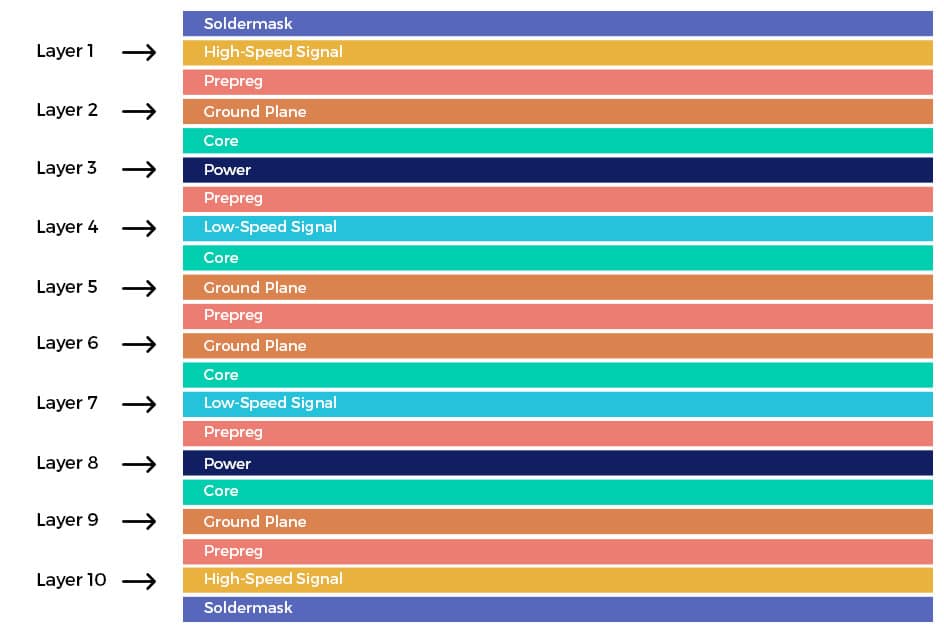
One PCB stackup example of a 10 layer PCB stackup is included below:
With the high operating speeds of modern circuits, careful PCB stackup design is necessary to improve distribution ability and limit interference. A poorly designed PCB may degrade signal transmission, producibility, power delivery, and long-term reliability.
Multilayer PCBs maximize the potential of circuit boards and provide exceptional opportunities for innovation. Trusting the design to a proven company is a wise decision for developing a quality electronic product.